Ⅰ. The introduction of PCB test
In order to ensure the quality of PCB production, manufacturers have gone through a variety of test methods during the production process, and each test method will be tested for different PCB defects. It can be divided into two categories: electrical testing method and visual testing method. The following will specifically introduce the types of PCB testing and PCB testing steps.
Ⅱ. Commonly used test methods for PCB
1. PCB manual visual inspection
Use a magnifying glass or a calibrated microscope, and use the operator's visual inspection to determine whether the circuit board is qualified or not, and to determine when the correction operation is required, which is the most traditional testing method.
Its main advantages are low upfront cost and no test fixture, while its main disadvantages are human subjective error, high long-term cost, discontinuous defect detection, and difficulty in data collection. At present, due to the increase in PCB production and the shrinking of the wire spacing and component volume on the PCB, this method has become increasingly infeasible.
2.PCB online test
Through electrical performance testing to find manufacturing defects and test analog, digital and mixed-signal components to ensure that they meet specifications, there are several testing methods such as bed-of-needle testers and flying probe testers.
The main advantages are the low test cost of each board, strong digital and functional testing capabilities, fast and thorough short-circuit and open-circuit testing, programming firmware, high defect coverage, and easy programming. The main disadvantages are the need to test fixtures, programming and debugging time, the high cost of making fixtures, and the difficulty of use.
3.PCB function test
The functional system test is to use special test equipment in the middle stage and the end of the production line to conduct a comprehensive test on the functional modules of the circuit board to confirm the quality of the circuit board. Functional testing can be said to be the earliest automatic testing principle. It is based on a specific board or a specific unit and can be completed with various equipment.
Functional testing usually does not provide in-depth data such as foot-level and component-level diagnostics for process improvement, and requires specialized equipment and specially designed test procedures. It is complicated to write functional test programs, so it is not suitable for most circuit board production lines.
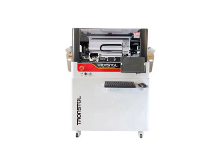
4. Automatic optical test
Also known as automatic visual testing, it is based on optical principles, comprehensively using image analysis, computer and automatic control and other technologies to test and deal with defects encountered in production. It is one of the newer PCB testing steps of confirming manufacturing defects.
5. Automatic X-ray inspection
Take advantage of the difference in X-ray absorption rate of different substances, see through the parts that need to be tested, and find defects. It is mainly used to test ultra-fine pitch and ultra-high-density circuit boards, as well as defects such as bridging, missing chips, poor alignment, etc. generated during the assembly process. It can also use its tomography technology to test internal defects of IC chips. The main advantage is the ability to test the quality of BGA soldering and embedded components without fixture cost; the main disadvantages are slow speed, high failure rate, difficulty in testing reworked solder joints, high cost, and long program development time. This is a relatively new test, and the method remains to be further studied.
6. Laser test system
It is the latest development of PCB testing technology. It uses a laser beam to scan the printed board, collects all measurement data, and compares the actual measurement value with the preset qualified limit value. Fast output, no fixtures and visual non-covered access are its main advantages; high initial cost, maintenance and use problems are its main disadvantages.
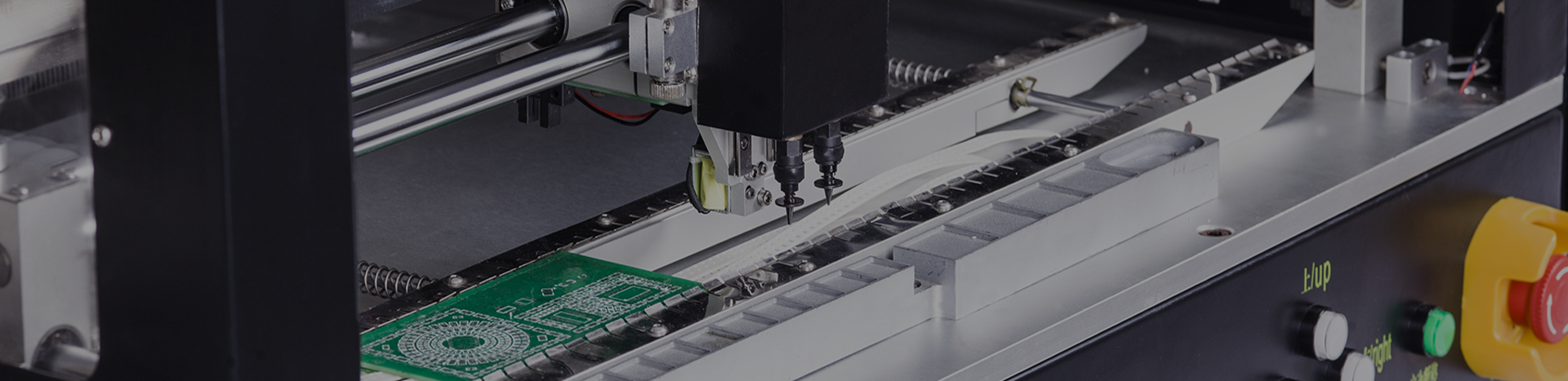
7. Size test
Use the two-dimensional image measuring instrument to measure the hole position, length and width, position and other dimensions. Since PCB is a small, thin and soft type of product, contact measurement can easily deform and cause inaccurate measurement. The two-dimensional image measuring instrument has become the best high-precision size measuring instrument.
 English
 日本語
日本語 한국어
한국어 français
 Deutsch
 Español
 italiano
 русский
 português
 العربية
 tiếng việt